PCB Assembly
Your trusted manufacturing partner for PCB assembly and beyond
Our end-to-end PCB assembly services are designed for consistent quality, seamless communication, and solutions customized to your exact requirements.
Our end-to-end PCB assembly services are designed for consistent quality, seamless communication, and solutions customized to your exact requirements.
Your product deserves nothing less than exceptional performance. With decades of experience in PCB assembly, we deliver the quality, functionality, and reliability you need for simple or complex designs. August Electronics serves as a single, integrated partner throughout the entire assembly process, streamlining your supply chain and shortening your time to market. From sourcing components to comprehensive testing, we manage every step of the assembly process, tailoring it to your project’s unique specifications. August isn’t just your contract manufacturer; we’re your manufacturing partner.
Our attention to detail and strict quality control exceed industry standards, elevating your product functionality and market appeal. Each unit is built to perform flawlessly, even in the most demanding environments. We work closely with you throughout your project, keeping you updated with clear, consistent communication and thorough documentation. With August, you can count on precision, transparency, and a trusted partnership from start to finish.
OUR CAPABILITIES
We support the assembly of single-layer printed circuit boards as a simple, high-quality solution for straightforward electronic applications. This option is perfect for low-complexity, cost-effective projects where reliability and accuracy are key. Whether your needs are basic or intricate, we bring consistent quality to all our assembly projects.
Our team is equipped to handle complex multi-layer boards that stack multiple layers of circuitry into one assembly. We deliver expertly assembled, high-performance multi-layer PCB assemblies built for demanding applications, including rigid and flex technologies to push your product capabilities further.
We offer through-hole technology (THT) assembly services for designs that require stronger mechanical bonds and long-term durability. Each connection is carefully soldered to meet industry standards and provide lasting reliability across all use cases.
Our Surface Mount Technology process leverages advanced placement systems to ensure high-speed, high-density builds for even the most intricate PCB layouts. With automated precision and experienced operators, we deliver the quality and consistency your projects demand.
We specialize in mixed assembly projects that combine through-hole and surface mount components on a single board. This hybrid approach allows us to meet your unique design specs with flexibility and accuracy, handling all the components your build requires with care.
MANUFACTURING PROCESS

Once we receive your files, our team leverages advanced software to send bid requests to thousands of suppliers. We consider availability, lead time, and cost to compile a detailed quote that includes PCB board assembly costs and any non-recurring engineering (NRE) expenditures.

Once received, our team uses advanced software to send bid requests to thousands of suppliers, factoring in availability, lead time, and cost. We then provide a detailed quote covering PCB board assembly costs and any non-recurring engineering (NRE) expenditures.

We meticulously source all the components or verify consigned materials, ensuring every item is in place. Each part is counted, logged, and checked against the BOM to meet your required quantity. Internally, we generate unique internal documentation for each build, assigning part numbers to every prepared PCB and component for full traceability and inventory control.

Next, we prepare the bare boards for surface-mount technology (SMT) assembly. Each PCB is labelled with a 2D barcode to track it throughout each assembly stage.
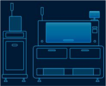
We apply solder paste using a solder paste printer and stainless steel SMT stencil derived from the Gerber files. A solder paste inspection (SPI) is performed to verify even distribution and alignment before components are placed.
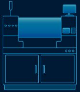
With the boards ready, components are loaded into feeders for our four SMT lines—two high-speed and two standard lines. Our pick-and-place machine accurately places SMT components onto the solder paste, setting the stage for the next step.

Before reflow soldering, we perform a pre-oven Automatic Optical Inspection (AOI) to validate polarity, spacing, placement, and markings, minimizing errors prior to the reflow stage.
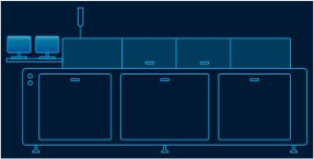
The boards are passed through a controlled reflow oven that heats them to optimal temperatures without compromising component integrity. This reflow soldering process is critical to forming strong joints and reliable solder connections.

Once cooled, we conduct a post-oven automated optical inspection (AOI) to identify any placement errors or defects. The inspection frequency is guided by panel quantity to balance precision and throughput.

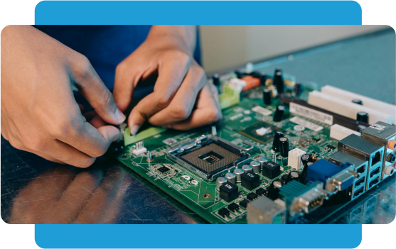
We use wave soldering and selective soldering machines (SSM) to ensure precise solder joints for assemblies requiring through-hole components. We can also handle mixed assembly projects, including SMT and through-hole components. Some complex or nonstandard parts are soldered manually for best results.

All boards go through a final inspection and are functionally tested based on customer requirements. Our inspection team verifies that each assembled board meets IPC standards before being approved for final shipment.

We manage custom packaging and delivery logistics, ensuring the assembled boards are securely packed and reach their destination securely and on time. Each order is tracked to maintain full visibility throughout the shipping process.
TESTIMONIALS
WHY AUGUST ELECTRONICS
With over 30 years in the industry, we bring the expertise and problem-solving skills to handle even the most challenging assembly projects. Our team’s extensive experience in PCBA services ensures that the job is done right.
We maintain tight control over quality, lead times, and costs by keeping all stages of the PCB manufacturing process under one roof. This integrated approach lets us quickly identify and resolve potential issues, providing a seamless experience.
We don’t believe in a one-size-fits-all solution. Our tailored services are designed to accommodate your specific needs, whether quick turnaround prototypes, low-volume runs, or scaling up for larger production.
Quality is a priority in everything we do. From day one, we’re committed to delivering durable, high-performance PCB assemblies that exceed your expectations.
Our rigorous testing strategies eliminate risks and ensure your product’s reliability. Every PCB assembly undergoes dielectric testing, functional testing, and AQL inspections to verify safety and functionality.
RESOURCE LIBRARY
CONTACT US
August Electronics is certified to ISO 9001:2015 and ISO 13485:2016, reflecting our commitment to quality in general manufacturing and medical device production. Our team also holds IPC certifications, including IPC-A-610 for electronic assemblies and IPC-7711/7721 for rework and repair. Additionally, we manufacture products that meet CSA, UL, and ETL safety standards and comply with Intertek, TÜV SÜV, and SGS international safety requirements. For more information, please visit our quality control page.
Our testing and inspection methods include 2D and 3D solder paste printing inspection (SPI), automated optical inspection (AOI), functional test, and X-ray testing for hidden defects. Our quality assurance processes also feature dielectric (Hi-Pot) testing and in-circuit testing to ensure your PCB assembly is secure, safe, and production-ready, down to the smallest copper trace or wire connection.
For consigned assembly projects where you provide components, we first validate each item to confirm compliance with our quality standards. From there, we integrate these components into our assembly process with the same attention to quality and accuracy as we would for components we source ourselves.
If a PCB fails during testing, we immediately conduct a root cause analysis to identify the issue. Depending on the nature of the defect, our corrective action could involve reworking the board, replacing defective components, or, if necessary, scrapping the board. We ensure the board complies with the original requirements before approving it for shipment.
We can attach components of a wide range of types, including surface-mount devices (SMD), THT components, and specialized components such as leadless package parts. We are also equipped to assemble complex boards involving assembling BGA and plated through-hole connections, using advanced soldering techniques for precision.