
What Does PCBA Stand For?
What Does PCBA Stand For?
You’ve seen the terms PCB and PCBA in emails, quotes, and file names for years without giving them a second thought. Someone sends over “PCB files,” another person asks for “PCBA pricing,” and the conversation keeps moving. As long as the boards arrive and the product works, the shorthand feels harmless.
The problem is that PCB and PCBA do not describe the same thing once you are actually building hardware.
One is a blank circuit board.
The other is a fully populated assembly that needed components, process time, and inspection to exist.
If that distinction is fuzzy, it becomes harder to scope work with a manufacturing partner, compare quotes, or understand where time and cost are really going in your product.
So what is a PCBA? This article explains how PCBA differs from a bare PCB, where it sits in the lifecycle of a product, and how, with August Electronics, the PCBA assembly process is one stage in the end-to-end manufacturing of electronic devices.
PCB vs PCBA Meaning: Board vs Assembled Board
What is a printed circuit board?
A PCB is the bare printed circuit board. It is a non-insulating base with conductive pathways, including the substrate material, copper traces, pads, vias, solder mask, and silkscreen that define the electrical layout of your design. At this point, you are dealing with Gerber files, drill data, stackup information, and board dimensions, but haven’t started mounting electronic components.
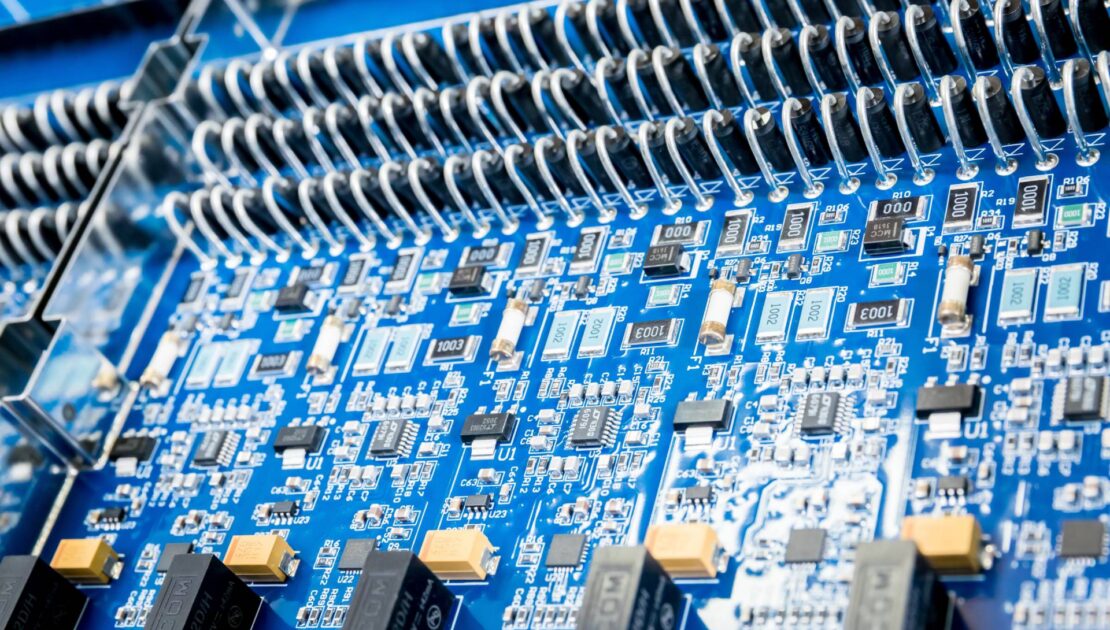
What is a printed circuit board assembly?
A PCBA is the same board after assembly. Surface-mount components have been placed and soldered in the reflow oven. Any required through-hole technology has been soldered. The result is a populated board that can be powered, tested, and integrated into a larger product. In other words, the difference between PCB and PCBA is whether the necessary electronic components are actually on the board.
Where PCBA Fits in the Product Lifecycle
You can think of the PCBA process as one link in a chain:
Before PCBA: Design and board fabrication
- Requirements, schematics, and PCB layout
- Component selection and DFM checks
- Bare PCB fabrication based on your stackup and drawings
PCBA: Turning the design into a working assembly
- Blank boards and critical components arrive at the line
- Solder paste application, surface mount technology (SMT) components are placed, and reflowed
- Any through-hole parts are added and soldered
- You now have a populated board that can be powered and tested to ensure optimal performance
After PCBA: Building the full product
- PCBAs are wired into cable and harness assemblies
- Boards are installed into box builds, enclosures, or control panels
- Final system checks, functional testing, packaging, and logistics complete the build
How a PCB Becomes a PCBA
At a high level, the PCBA manufacturing process looks like this:
Material preparation
Bare PCBs and all the components arrive and are checked against the build documentation. This is where board revisions, BOM versions, and special handling notes are confirmed, so the line is working from the correct set of instructions.
Solder paste application
Solder paste is printed onto the PCB pads using a stencil that matches the layout. The quality of this step affects how well components solder later, so paste volume and alignment are controlled closely.
Surface mount placement
Pick-and-place equipment positions surface mount components on the pre-pasted pads. This includes active and passive components. Component placement accuracy is key to good solder joints and reliable assemblies.
Reflow soldering
The populated boards go through a reflow oven, where molten solder creates permanent electrical connections between component leads and pads. When the boards exit, the SMT side is fully soldered.
Adding through-hole parts
If the design includes through-hole components, they are added after reflow. These parts are attached either manually or with selective or wave soldering, depending on the build and volume.
Initial inspection
A completed assembly undergoes quality control inspections to catch issues early. Automated optical inspection (AOI) is used to check placement and solder joints, supported by visual checks where they make sense for the product.
The details behind each of these steps can change with product, volume, and technology, but the goal is the same: a consistent way to turn design data into repeatable, buildable assemblies.
How August Supports Your Next PCBA Project
August supports OEMs across a wide range of applications, including consumer electronics, oil and gas, industrial equipment, power and renewables, communications, and medical devices. That mix shapes the entire process, because the same assembly approach will not serve consumer electronics, a downhole tool, and regulated medical devices equally well.
You can come to August Electronics with an existing PCB assembly layout, a product you are moving from another electronics manufacturing company, or a device that has outgrown hand-built boards. We can translate that into an assembly process that makes sense for your volumes, component mix, and downstream integration, rather than treating PCBA as an isolated task.
If you are planning the next revision of a product, preparing to ramp something that currently lives on the lab bench, or consolidating how your electronics are built, reach out to August Electronics to start a conversation about how PCBA fits into your overall build.